




Technical Paper Overview
Wafer Surface Analysis: Detecting Defects With Laser Solutions Catching a wafer defect early depends on a laser that holds steady power and beam quality 24/7.
Semiconductor wafers are inspected for surface defects at every stage of manufacturing, and at least three times: when the wafer is created, at incoming quality control at the chip plant, and during and after development of the microchips. Any surface defect renders a chip unusable, so many of these inspections use lasers for their measurement precision and resolution. Laser light is rapidly scanned across the wafer’s surface or edge with a high-speed polygon scanner, and any deviation in the reflected light indicates a defect.
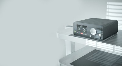
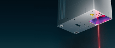
This white paper covers what that demands of the laser: long lifetime, maintenance-free operation, passive water-free cooling, controlled speckle patterns, exceptional beam quality, zero power fluctuation, and the resolution to image ever-smaller features. It then shows how Laser Quantum’s axiom LE addresses them: a 12 W air-cooled laser that avoids the liquid cooling widely prohibited in this application, with a customized bandwidth profile for the inspection’s speckle pattern, active noise suppression, and integrated power feedback.
Key takeaways include:
- Why wafers are inspected at least three times, and why one surface defect can make scrapping a wafer early cheaper than running it through the rest of the process
- How laser wafer inspection works: a high-speed polygon scanner sweeps the beam across the wafer surface or edge, and changes in the reflected light flag defects
- The seven laser requirements that make deployment hard: long lifetime, maintenance-free operation, passive water-free cooling, controlled speckle, exceptional beam quality, zero power fluctuation, and smaller-feature imaging
- Why air cooling matters: liquid cooling is widely prohibited in this application, and the axiom LE delivers 12 W without it
- What a customized bandwidth profile, active noise suppression, and integrated power feedback add: a speckle pattern tuned to inspection and a beam specification that holds with no power fluctuations, plus remote maintenance and service access
Download the full white paper for the complete list of laser requirements, the three-stage wafer inspection process, and a closer look at how the axiom LE’s air-cooled design, customized speckle profile, and integrated power feedback support 24/7 wafer inspection. Then talk to an application engineer about the laser your inspection system needs.