


Advanced Industrial
Electronics &
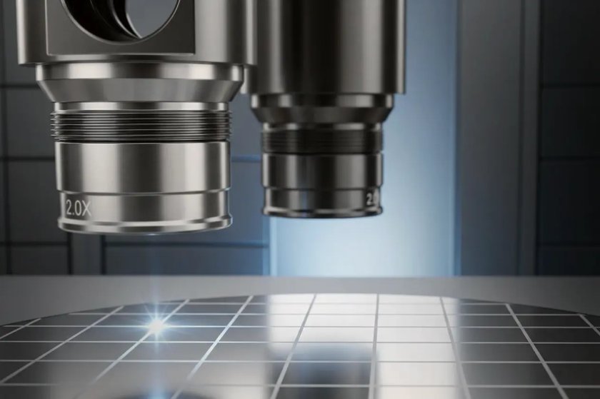
Semiconductor Laser Processing
Semiconductor equipment manufacturers rely on tightly integrated laser sub-systems to meet the accuracy, throughput, and reliability demands of advanced device fabrication.

Enabling Semiconductor Laser Processing System Performance
Semiconductor laser processing tools operate under increasing pressure to deliver higher precision, greater throughput, and tighter process windows, while supporting shrinking feature sizes and advanced materials. Equipment manufacturers must balance accuracy and speed with uptime, repeatability, and integration into tightly controlled fab environments.
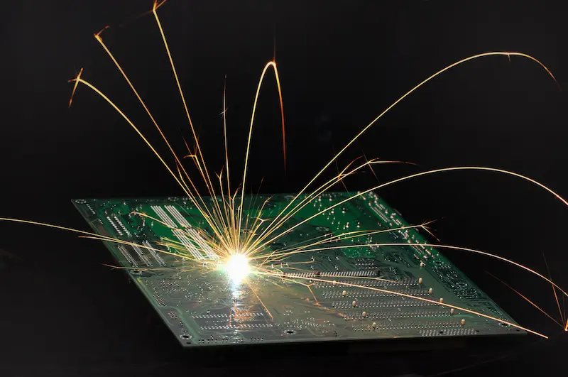
Supporting Laser Via‑Hole Drilling and Micro Machining
Applications such as laser via‑hole drilling and micro machining require precise control over laser energy delivery and beam motion to achieve consistent feature geometry across wafers and panels. Equipment builders must coordinate laser output, scan dynamics, and motion systems to maintain uniformity at high processing speeds.
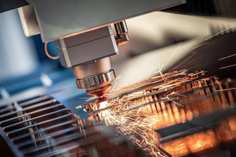
Precision Beam Steering for Wafer Dicing and Laser Dicing
Wafer dicing and laser dicing processes demand accurate, repeatable beam placement across large substrates, often at high line speeds. Multi‑axis scan heads and polygon scanners play a critical role in maintaining edge quality, positional accuracy, and throughput.
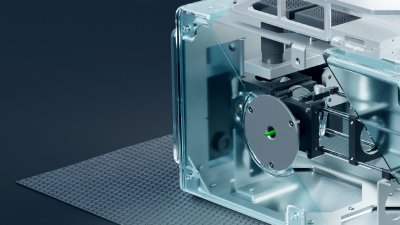
Designed for Semiconductor Tool Integration
Semiconductor equipment manufacturers must design tools that meet stringent requirements for cleanliness, reliability, and serviceability, while fitting within constrained mechanical and optical envelopes. Photonic sub-systems must integrate seamlessly with tool controls, motion stages, and factory automation.
Our advanced technologies are designed to support semiconductor machine builders developing and scaling laser‑based processing platforms, where precise energy control, deterministic beam positioning, and long‑term operational stability are critical to process consistency and tool performance.
Advantages of Semiconductor Laser Processing Enablers
The benefits of Semiconductor Laser Processing include:

Stable laser output
Supports consistent material interaction across wafers and process steps.

Accurate beam positioning
Enables repeatable feature placement and controlled edge definition.

High‑speed scanning capability
Supports throughput requirements for dicing and micro machining tools.

System‑level integration
Advanced technologies designed to align with semiconductor tool architectures.
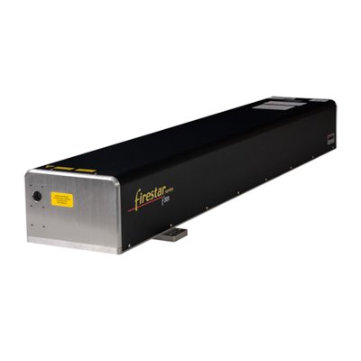
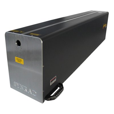
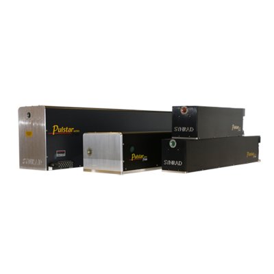
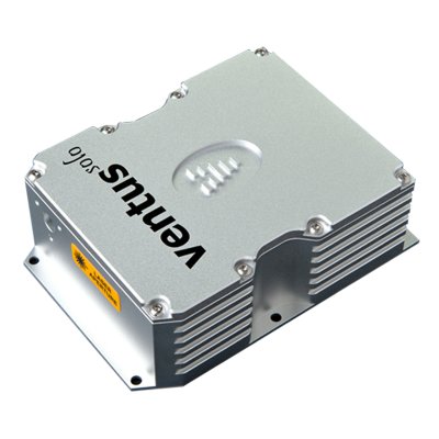
Related Products
Related Content


Request an Application Test
Engage with our team to evaluate laser, beam steering, and scanning technologies within your laser additive manufacturing system architecture.