
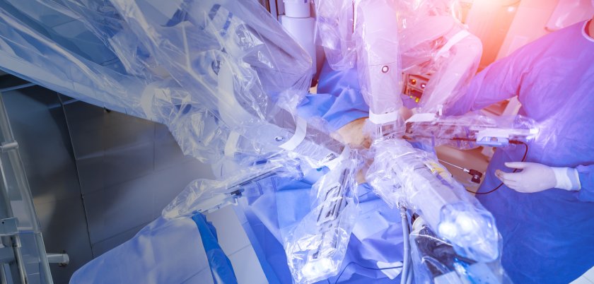
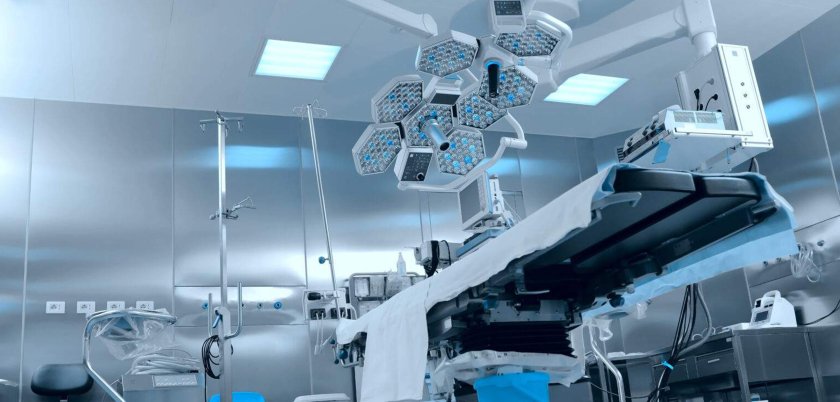
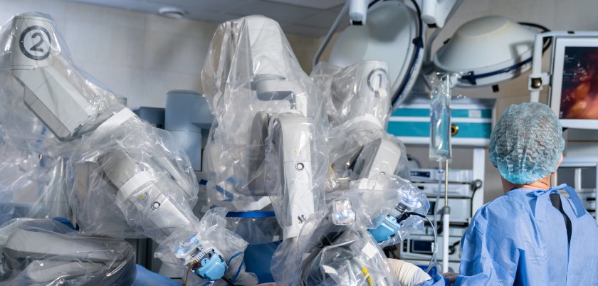

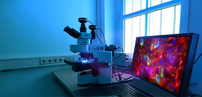
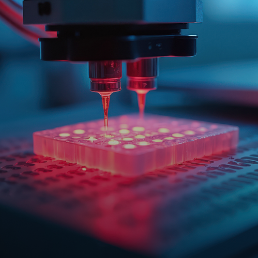

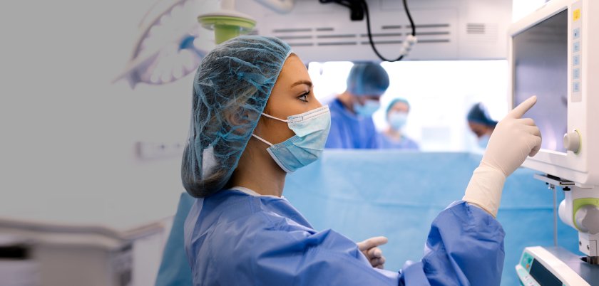


Precision Medicine
Semiconductor Solutions
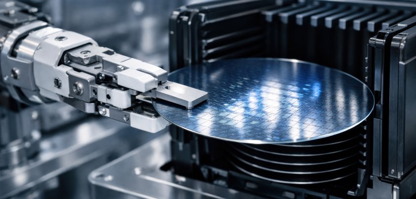
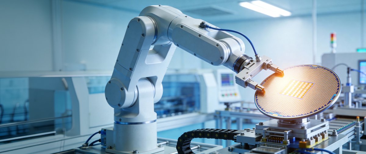
Semiconductor manufacturing requires extreme precision and control at every stage, from wafer handling to advanced lithography. This document highlights solutions that deliver ultra-precise motion, real-time feedback, and contamination-resistant designs to ensure high yield and reliability in cleanroom environments.
Modern semiconductor systems demand more than advanced tools. They require integrated process control, precise material handling, and high-resolution inspection to maintain consistency at smaller nodes, with every stage operating at high accuracy and stability.
Semiconductor Innovation
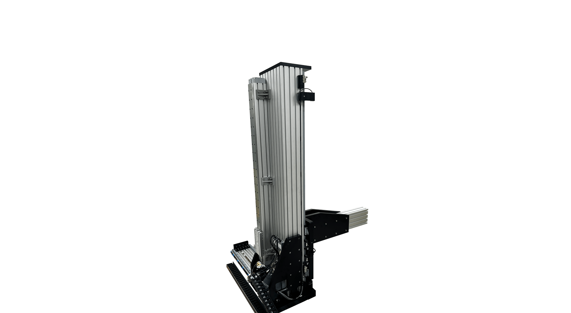
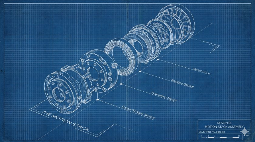
Z-Axis Vertical Stage
Tall central structure providing precise vertical motion for lift and positioning.
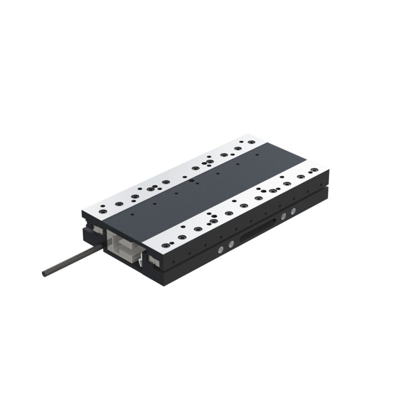
X-Axis Linear Stage
Base-mounted horizontal stage enabling lateral movement across the system.
Moving Carriage / Crosshead
Interface between X and Z axes that carries the payload or end effector.
End Effector Mount
Mounting point for wafer holder or process tooling.
Semiconductor Technology
Ultra-Precision Motion for Wafer Processing
Semiconductor manufacturing demands extreme accuracy at every stage. Our high-resolution encoders and motion control solutions enable precise positioning for wafer handling, lithography, and inspection processes. This ensures consistent alignment, reduced defects, and optimal yield across advanced nodes.
Sub-Nanometer Resolution for Advanced Nodes
As device geometries shrink, precision becomes even more critical. Our advanced encoder technology delivers sub-nanometer resolution, enabling accurate motion control for cutting-edge semiconductor applications, including EUV lithography and high-density packaging.
Real-Time Feedback for Process Control
Our solutions provide real-time position and motion feedback, allowing semiconductor equipment to maintain tight process tolerances. With high-speed data acquisition and low-latency response, manufacturers can achieve greater control over critical fabrication steps, improving throughput and reliability.
Thermal Stability for Consistent Performance
Temperature fluctuations can impact accuracy in semiconductor processes. Our thermally stable designs minimize drift and maintain consistent performance over long production cycles, ensuring reliable operation in high-throughput manufacturing environments.
Contamination-Resistant Design for Cleanroom Environments
Built for stringent cleanroom standards, our encoders are designed to minimize particle generation and withstand controlled environments. Materials and construction methods support ISO-class cleanroom requirements, helping maintain purity throughout the semiconductor fabrication process.
Scalable Solutions for Complex Semiconductor Systems
From front-end wafer fabrication to back-end assembly and test, our solutions integrate seamlessly into complex semiconductor equipment. Designed for scalability and interoperability, they support evolving manufacturing requirements and next-generation technologies.
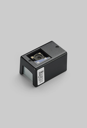
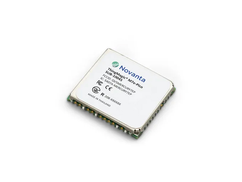
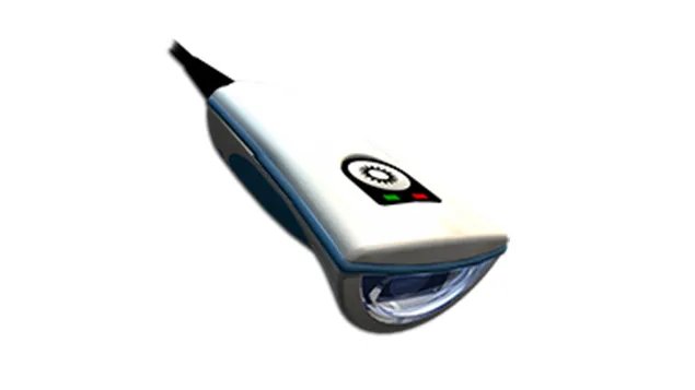
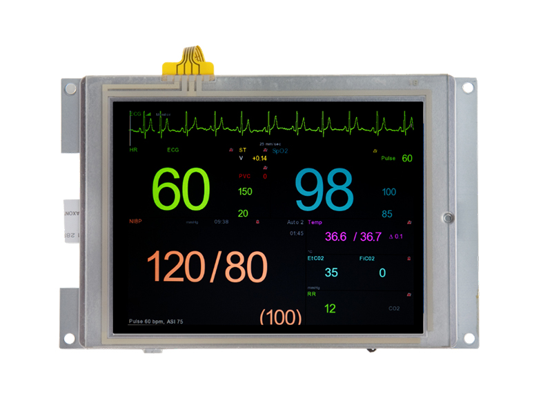
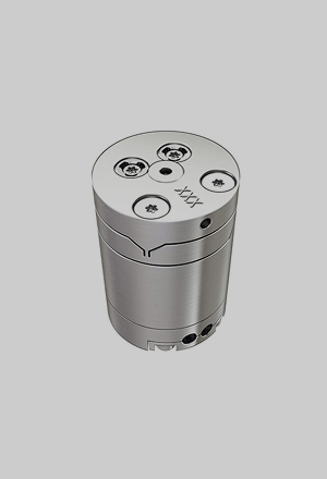
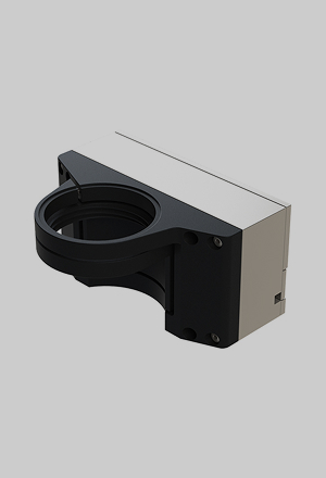
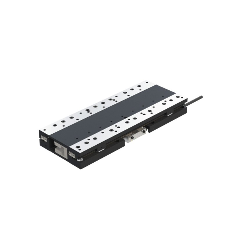
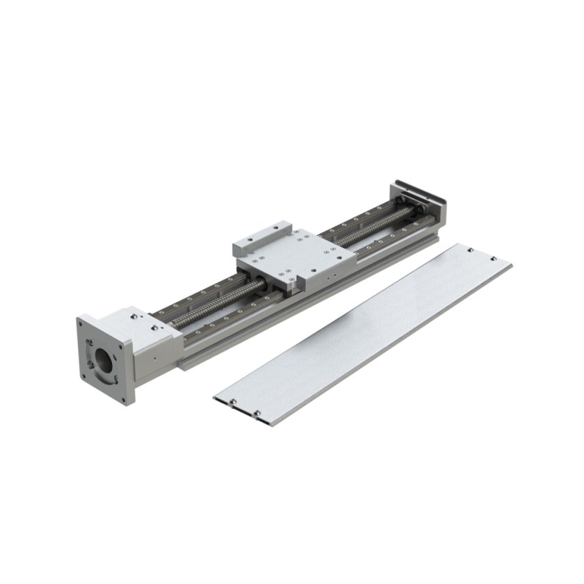
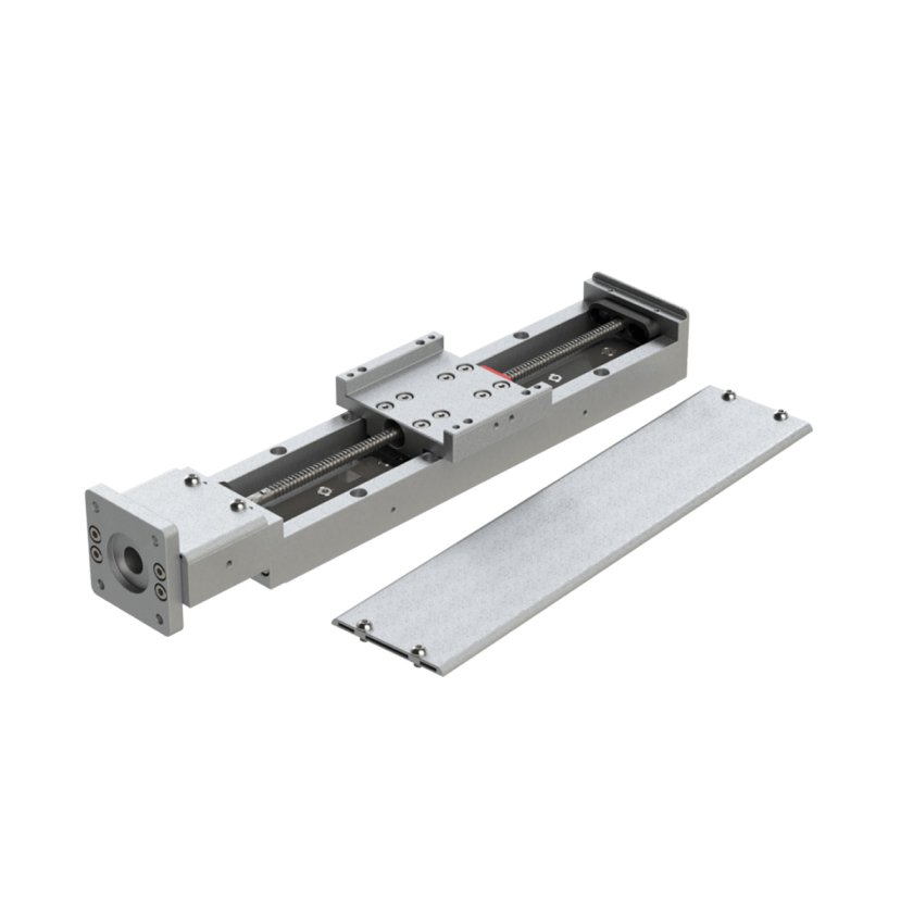
Our Products For Semiconductor Technology

Explore Our Semiconductor Applications

Contact Us
This consultative sales style, combined with our family of standard and customizable products, ensures that you always get the best product for your application.